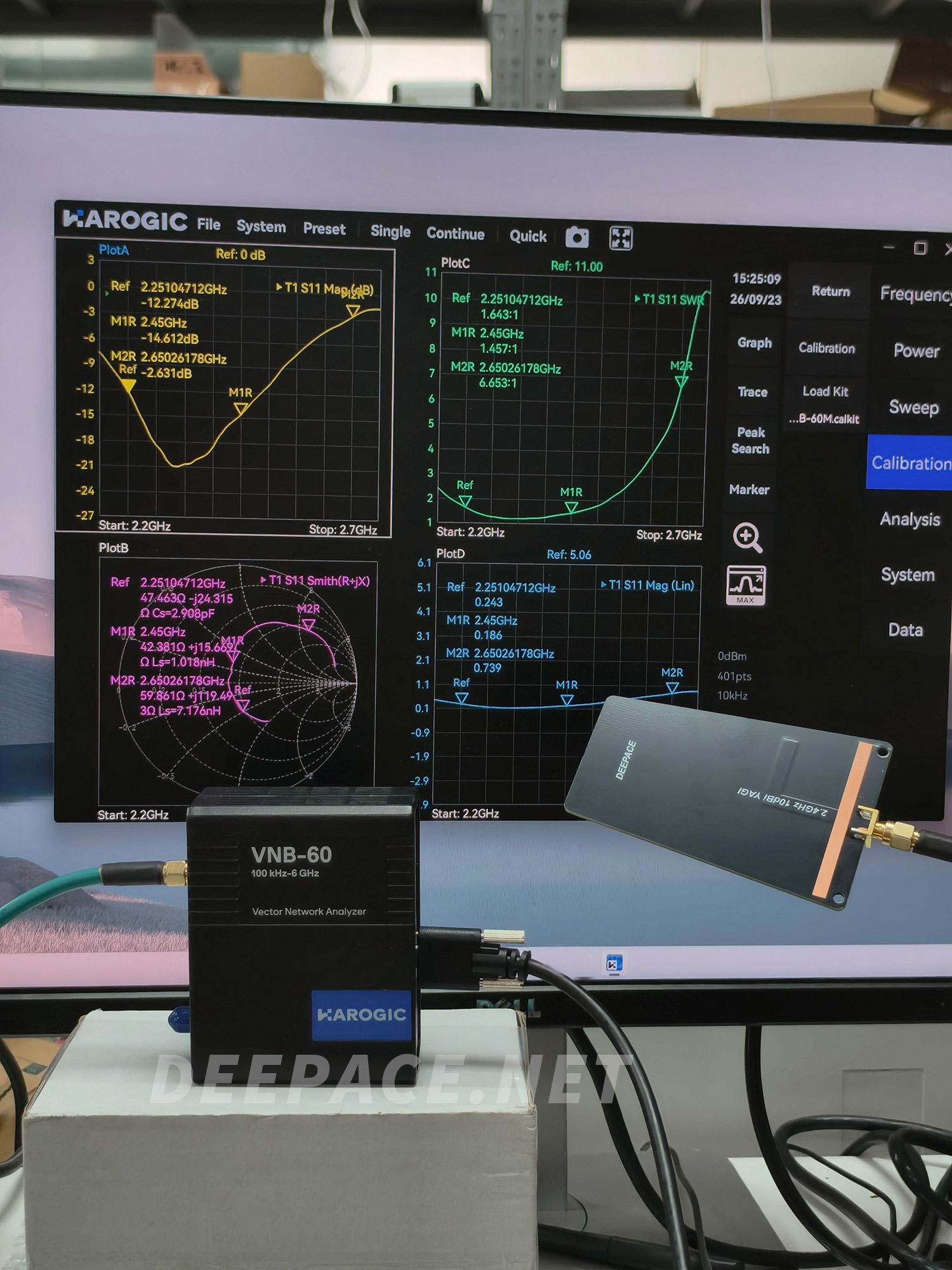
Harogic has introduced its first vector network analyzer, the VNB60, packing two-port measurement capability into a remarkably compact enclosure. Today, we take a brief look inside to explore its mechanical construction and circuit design.
Exterior and Mechanical Construction
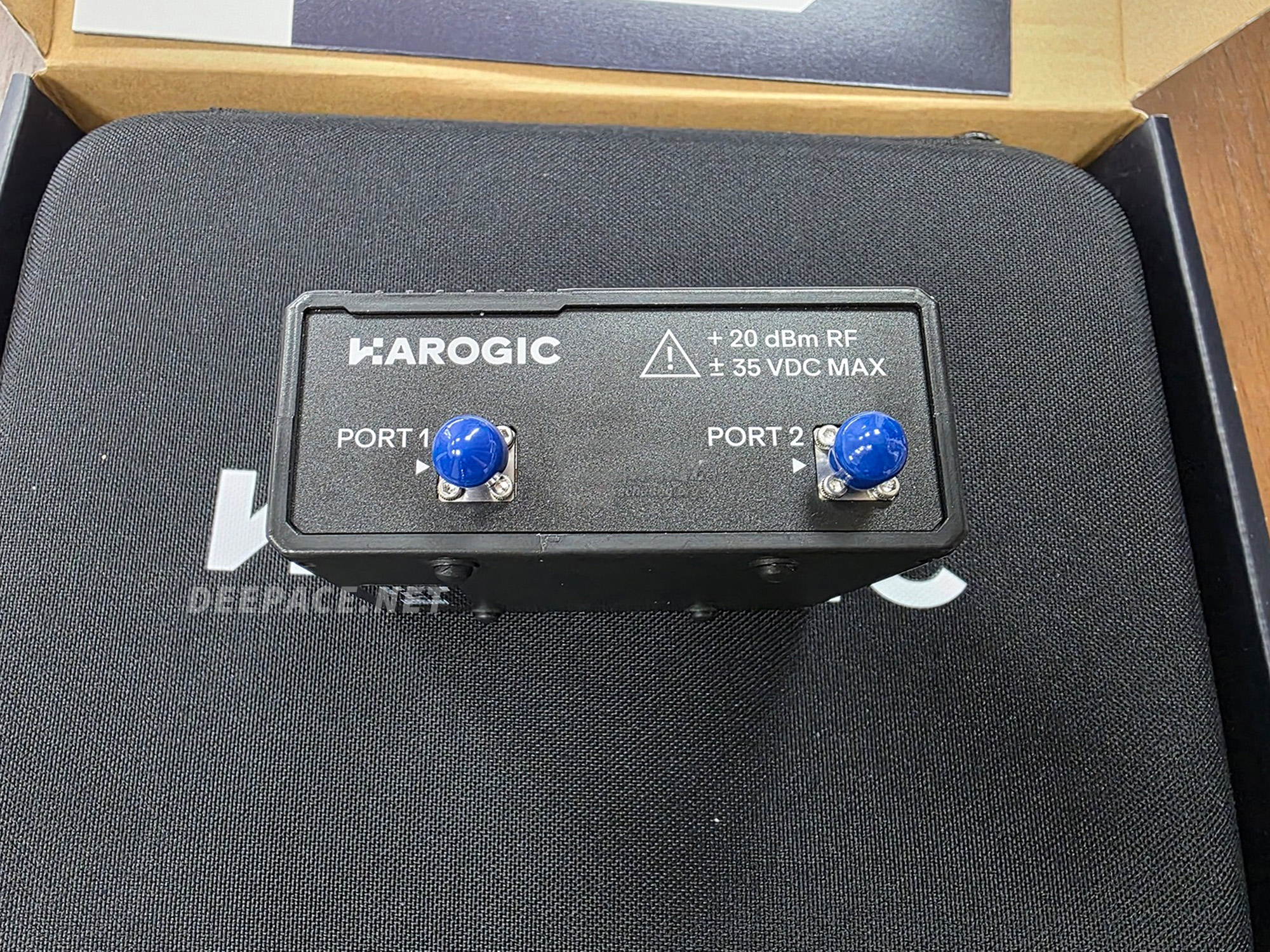
The VNB60 is smaller than the palm of a hand, with two RF measurement ports on the front and a USB Type-C port and auxiliary connector on the rear.
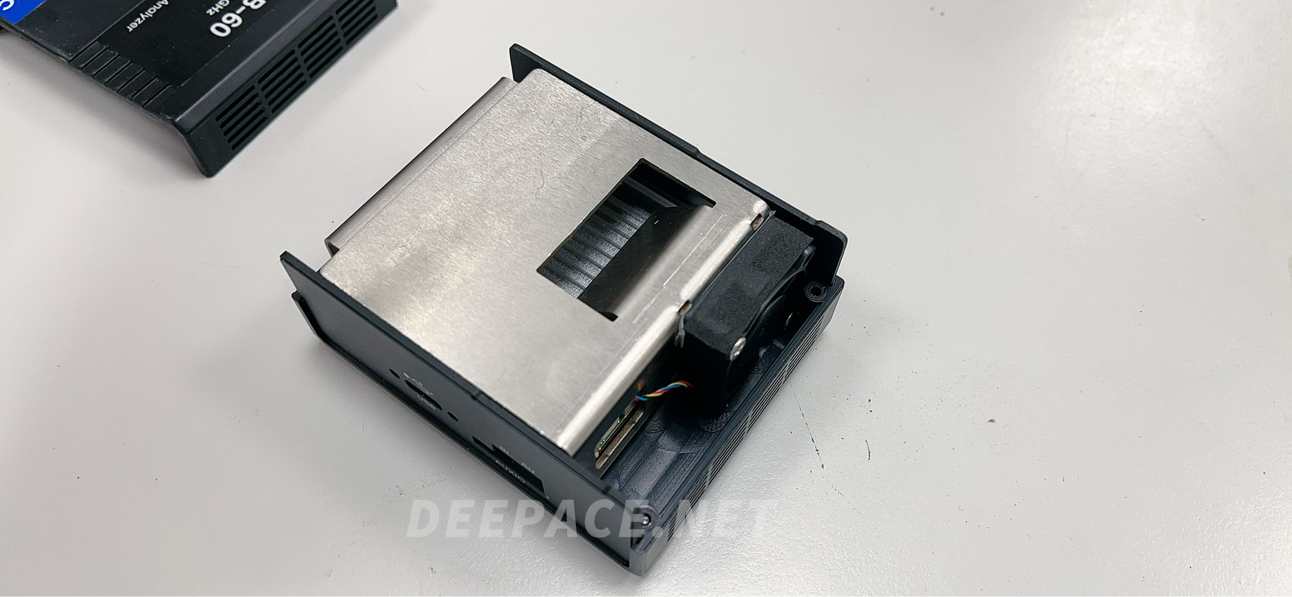
Opening the enclosure reveals a sturdy sheet-metal bracket that supports and secures the measurement module. A fan is mounted on the side, and the bracket incorporates an air duct that directs airflow into the module. This arrangement combines mechanical support with cooling, helping reduce heat buildup inside. In RF measurement instruments, temperature changes often cause amplitude and phase drift, making thermal design an important consideration.
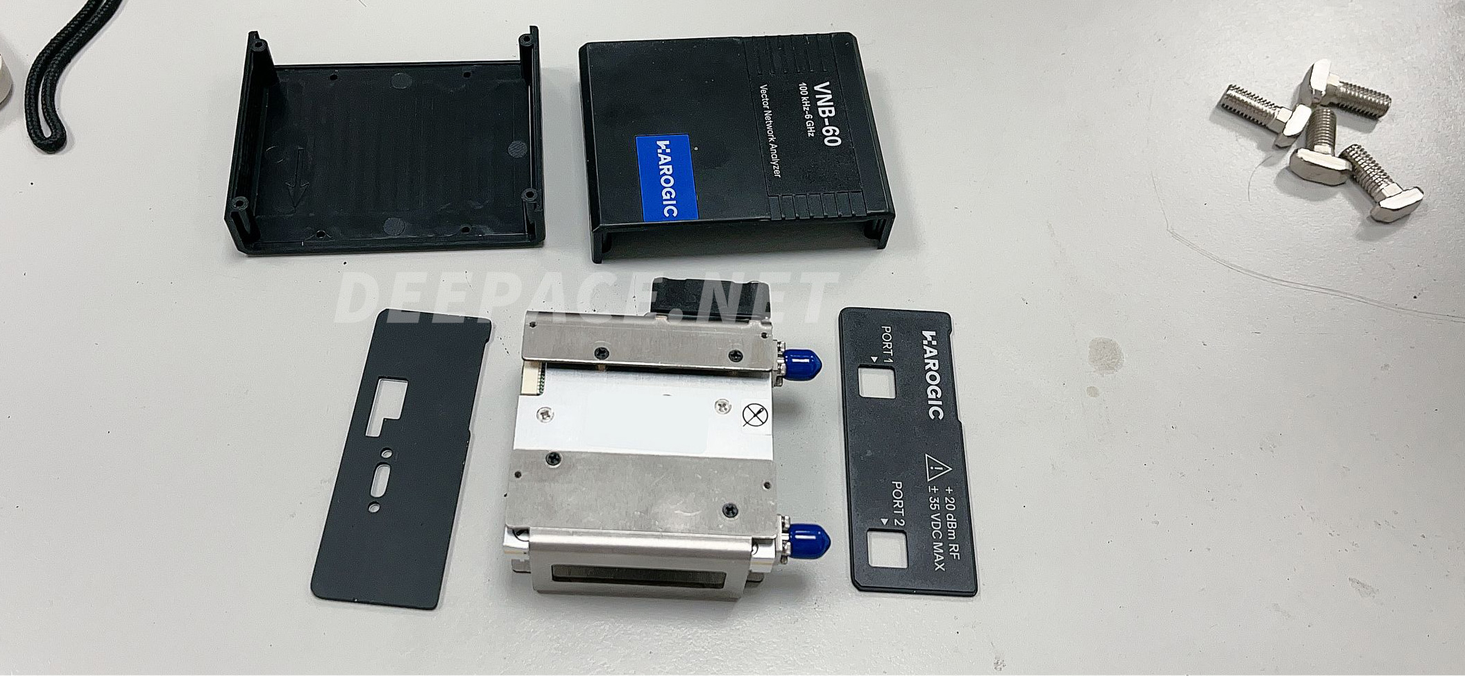
Lifting out the internal assembly shows that the measurement module is supported by the bracket with clearance around it inside the enclosure. Removing the mounting screws and disconnecting the fan cable reveals the module itself.
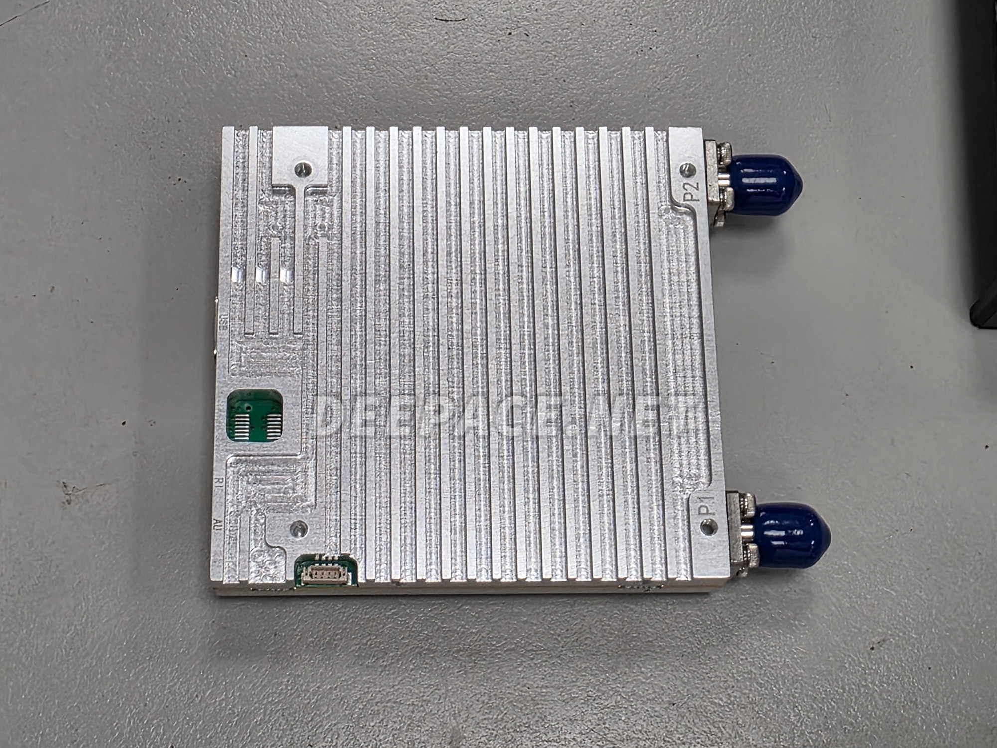
The module uses a sandwich construction, with a single PCB held between upper and lower aluminum shielding housings. Removing the top screws and housing exposes the circuitry.
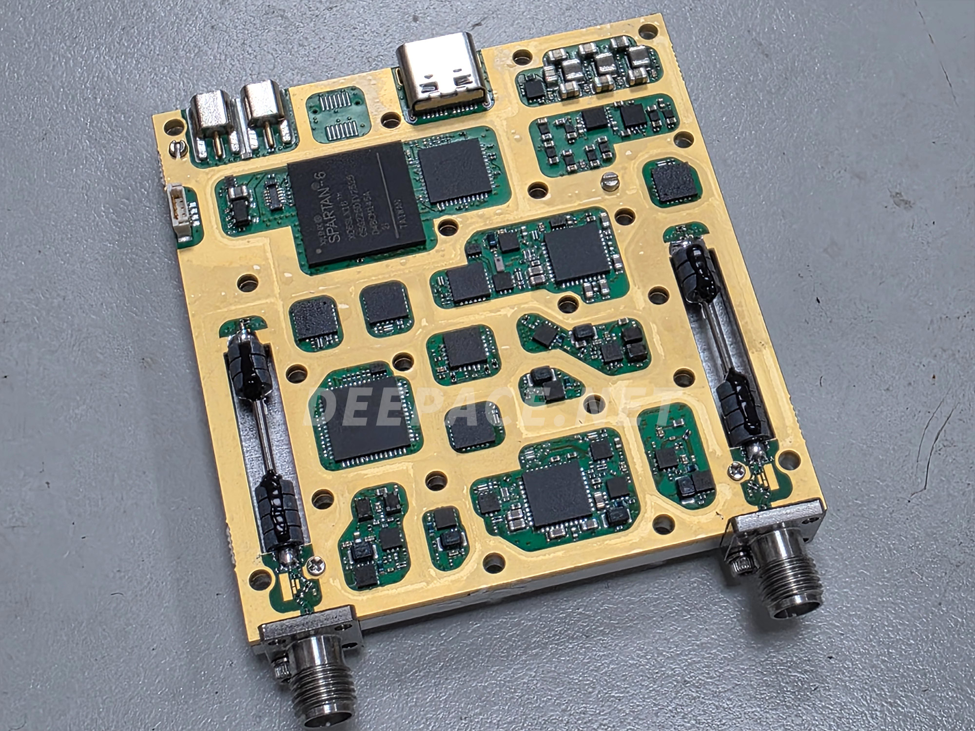
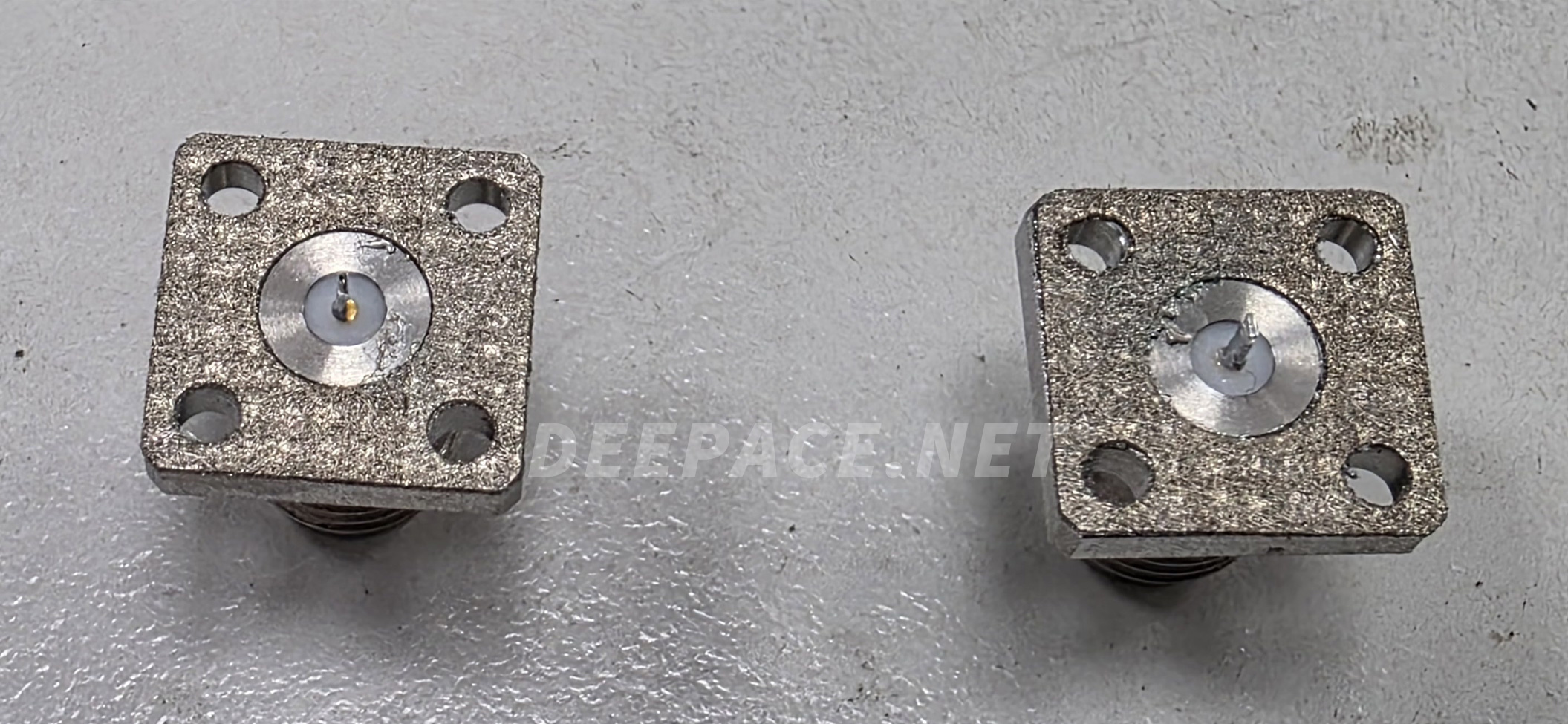
Custom SMA connectors are soldered directly to the PCB’s microstrip transmission lines. Desoldering and removing the connectors reveals conductive material at their contact surfaces to improve electrical contact and grounding. Conductive material is also used where the shielding housings meet the PCB, strengthening electrical continuity and shielding effectiveness.
Circuit Analysis
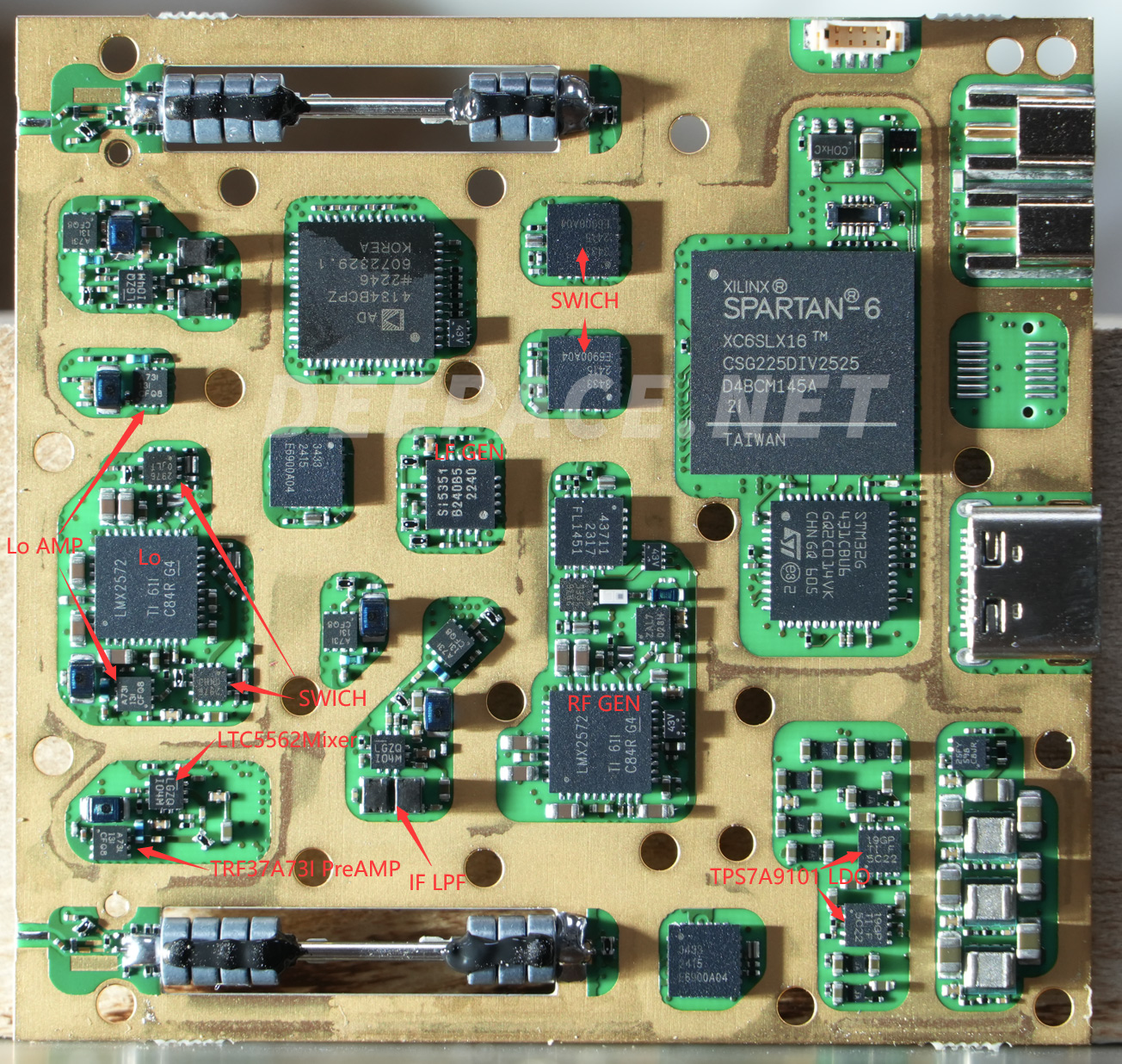
Two directional couplers built from coaxial lines and ferrite cores immediately stand out on the board. These are key components of the VNA’s RF front end, separating signals traveling in opposite directions. The receiver system then compares the amplitude and phase of the measurement signals against the reference signal to determine the corresponding S-parameters.
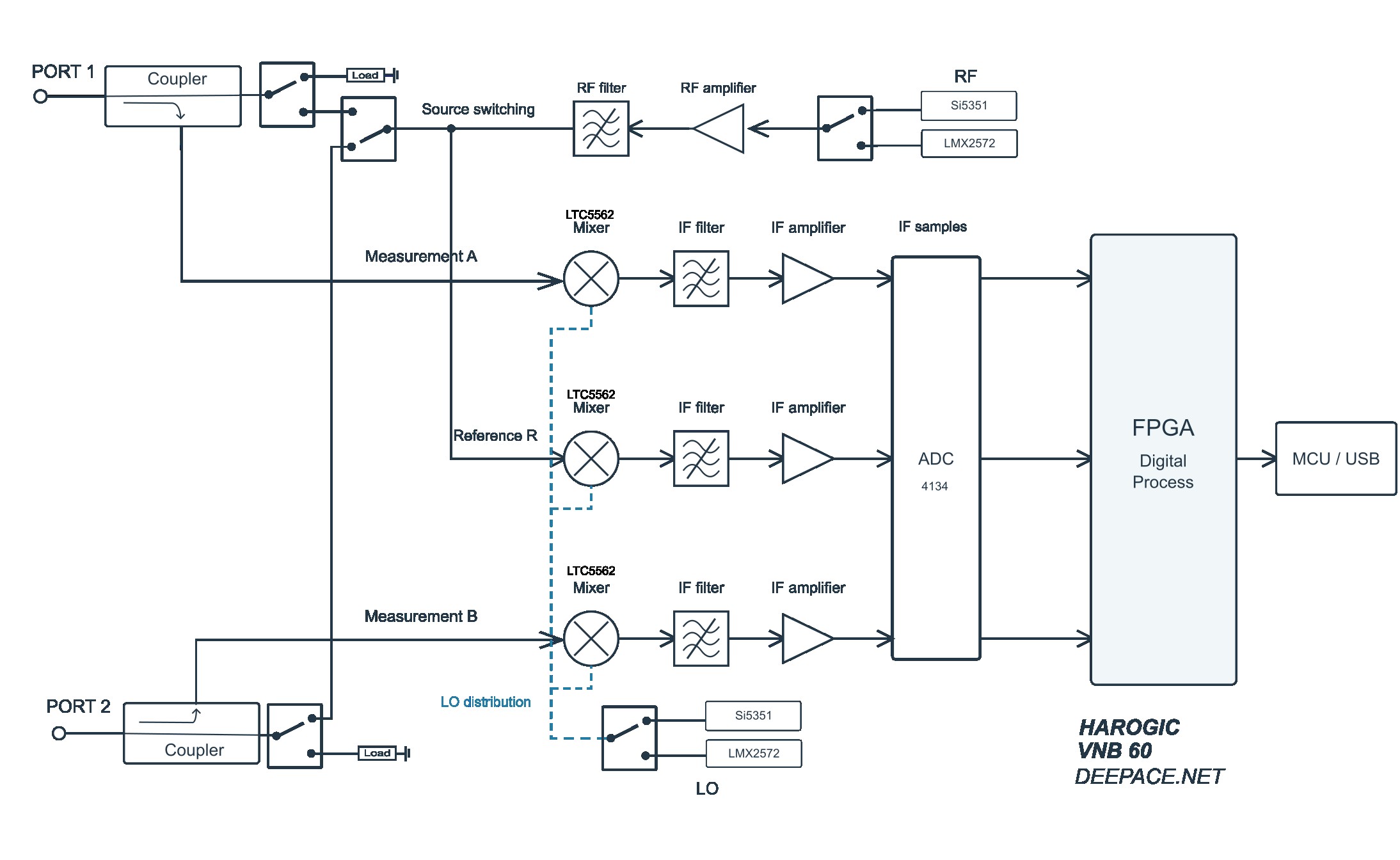
The mixer circuits sit close to the couplers. Based on our teardown observations, the VNB60 uses a single-conversion architecture with three receiver channels. The RF signals are mixed with the local oscillator (LO) signal, then pass through IF filtering and related circuitry before being sampled by the ADC. The digital signals are processed in an FPGA, while an MCU handles USB communication with the host computer.
We have drawn a simplified block diagram of this signal path to help illustrate how the instrument works.
Comparison with the KC901K Network Analyzer
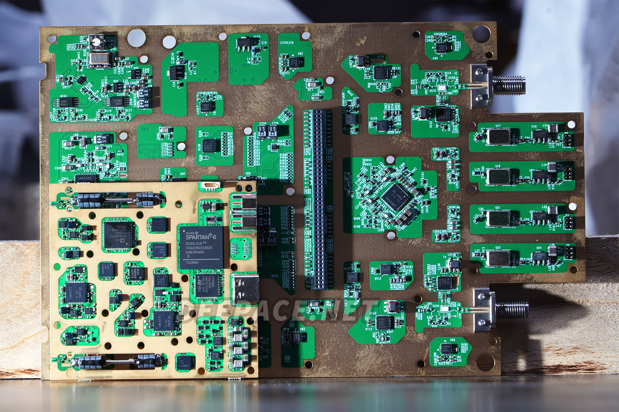
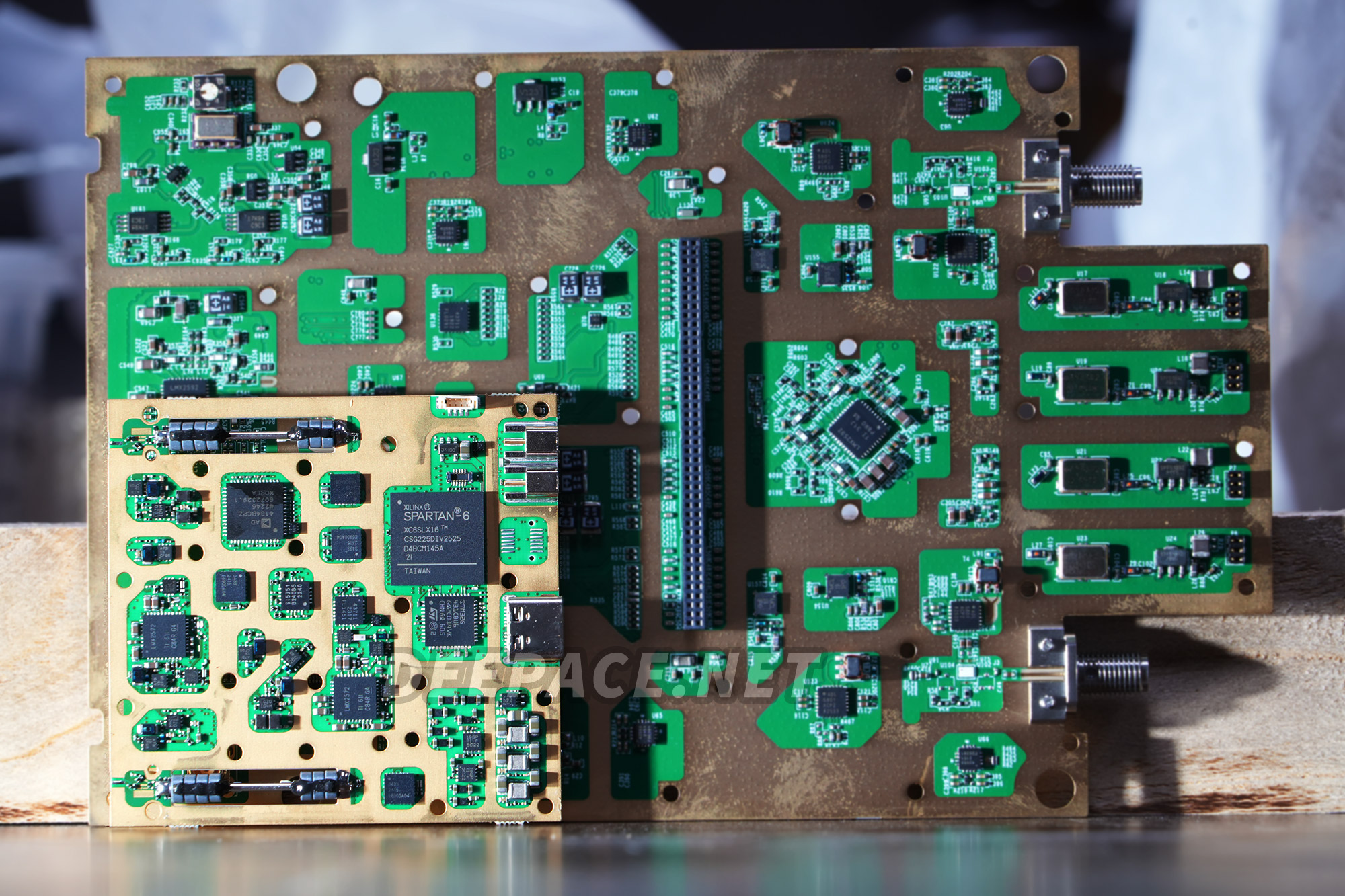
The KC901K provides an interesting comparison. Both instruments cover frequencies up to 6 GHz, while the KC901K extends down to 1kHz and the VNB60 starts at 100 kHz. Placing their circuit boards side by side makes the size difference clear: the KC901K has a larger main PCB, with its IF processing circuitry distributed across multiple boards., while the VNB60 uses a more compact layout.
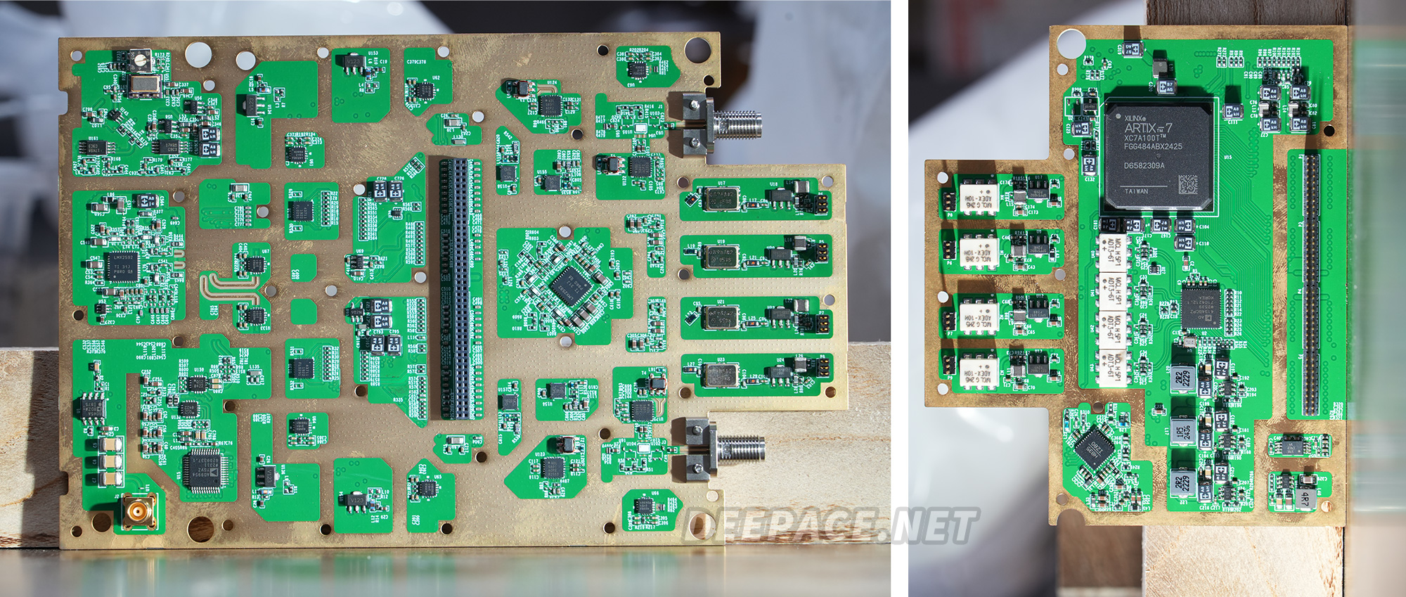
RF and IF boards of the KC901K.
Their receiver architectures also differ. The VNB60 uses a single-conversion architecture with three receiver channels, whereas the KC901K uses a dual-conversion architecture with four receiver channels.
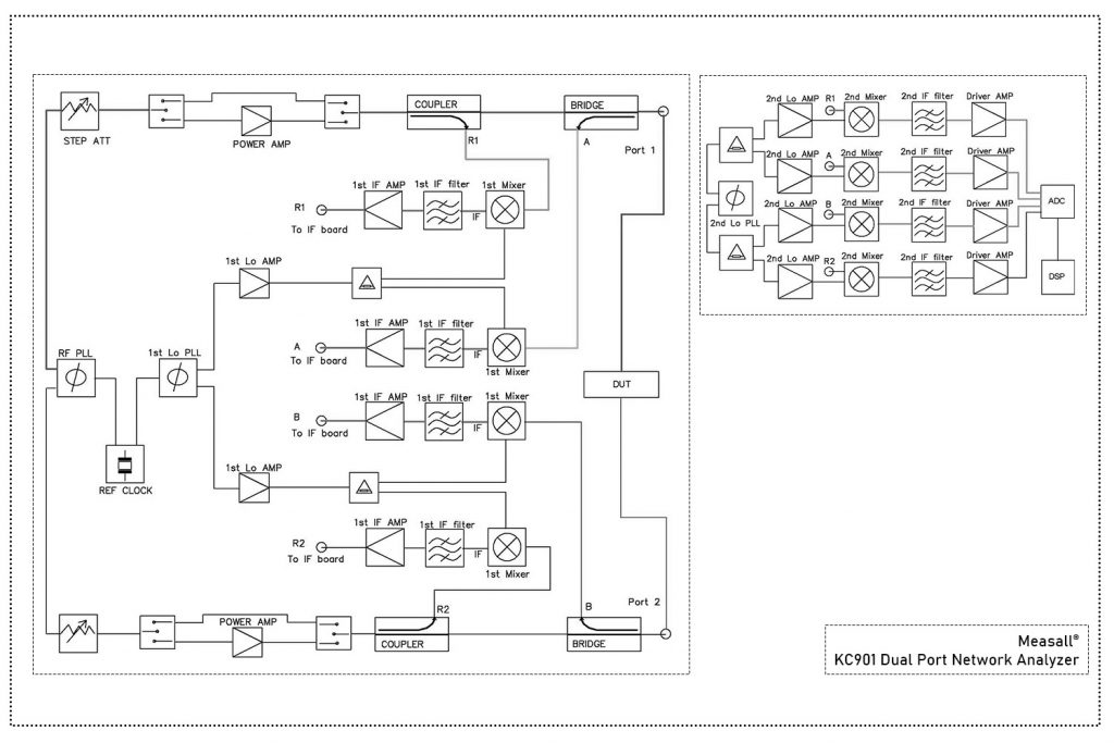
Single conversion reduces the number of conversion stages, helping shorten the signal chain and reducing the number of stages whose gain and phase stability must be managed. The KC901K follows a more traditional dual-conversion approach, with additional IF circuitry and relatively bulky crystal filters visible in the IF signal path. This implementation requires more board space and contributes to higher power consumption. The VNB60’s single-conversion approach is well suited to a compact USB instrument, achieving impressive dynamic range and low noise in an exceptionally small package—a result that reflects a high standard of RF design.
Final Thoughts
The VNB60 combines a remarkably compact footprint with thoughtful mechanical and RF design. Its single-conversion architecture keeps the signal path short, providing a sound basis for good RF performance while fitting the requirements of a compact laboratory instrument.
In our initial use, we found it well designed, with responsive sweep speeds and the capabilities needed for a wide range of component measurements, including filters, antennas, and cables. Support for the ECB-60 electronic calibration module adds convenience by simplifying routine calibration.
With its small size, reasonable price, and convenient USB connectivity, the VNB60 is an attractive choice for a PC-based RF workbench. We recommend it to users looking for a compact and capable two-port VNA.