Overview
The Harogic SAN-45 is a compact USB-powered spectrum analyzer and receiver covering a frequency range from 9 kHz to 4.5 GHz.
According to manufacturer specifications, the instrument provides:
- Analysis bandwidth up to 50 MHz (optional 100 MHz)
- Sweep speed exceeding 1 THz/s (RBW = 250 kHz)
- Typical phase noise of approximately –110 dBc/Hz at 1 GHz (10 kHz offset)
- Displayed average noise level (DANL) around –168 dBm/Hz with preamplifier enabled
- USB 3.0/2.0 Type-C interface, designed for operation with Windows and Linux PC software
This article presents a teardown-based analysis focusing on hardware architecture and implementation.
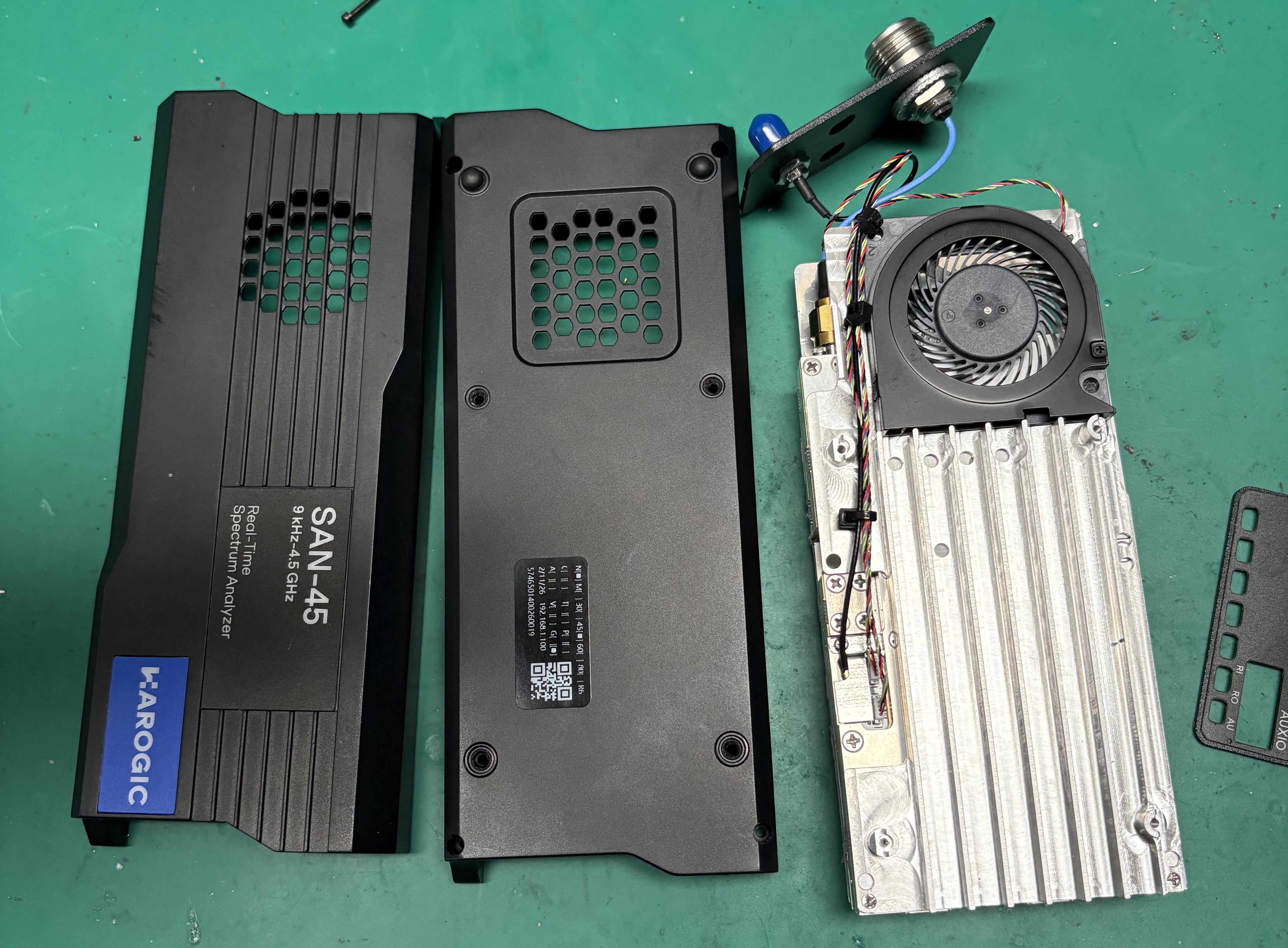
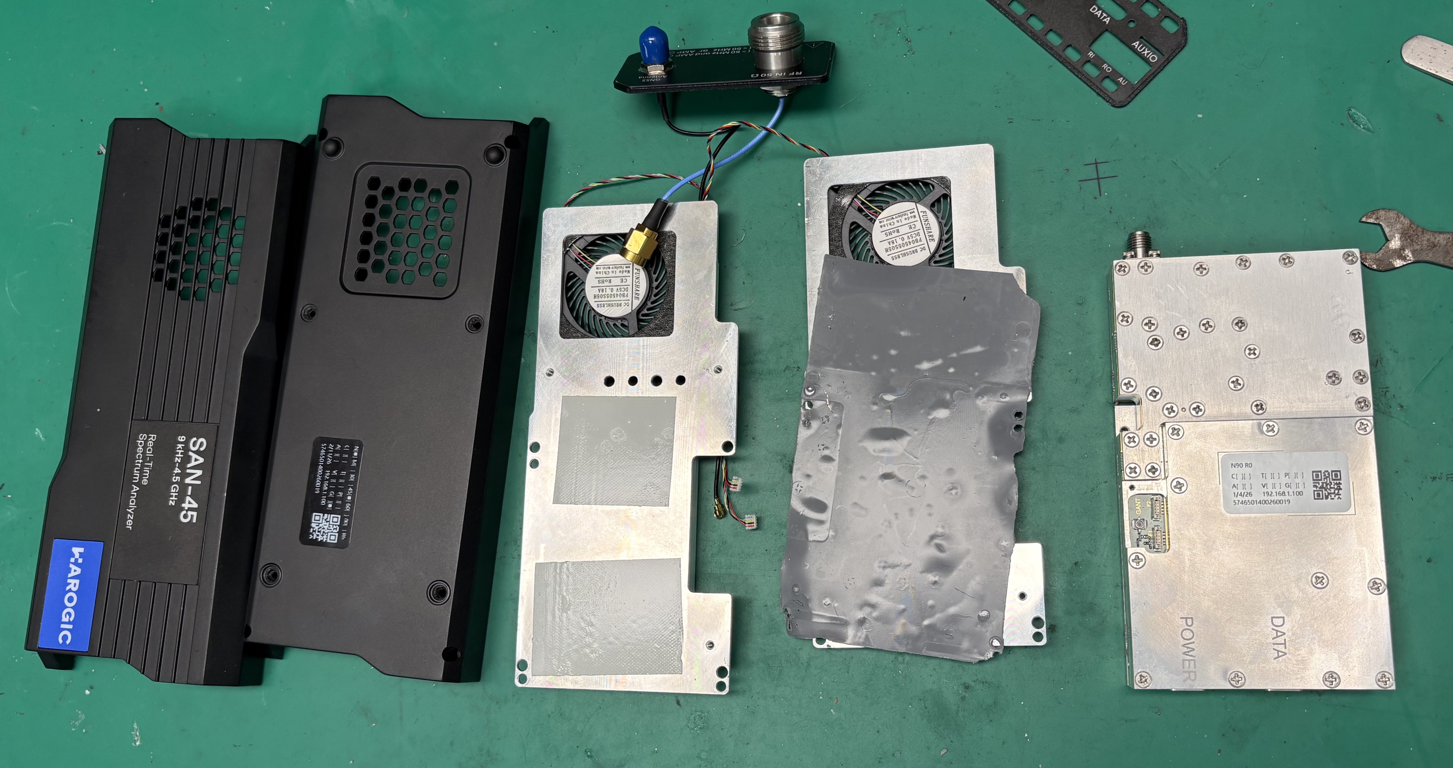
Mechanical Structure and Thermal Management
The device is housed in a two-piece black plastic enclosure with integrated ventilation openings.
After removing the enclosure, the core instrument assembly becomes visible:
- A machined aluminum chassis supports multiple stacked PCBs
- Aluminum heat spreaders are installed on both the top and bottom sides
- Each side includes a small centrifugal (blower-style) cooling fan
- Thermal interface materials (TIM), such as thermal paste or gap fillers, ensure direct contact between heat-generating components—especially the RF core—and the heatsinks
Once fully disassembled, the RF module itself is revealed to be highly compact, roughly comparable to the size of a credit card. This highlights a high level of integration within a relatively small footprint.
RF Front-End Architecture (PCB 1 & PCB 2)
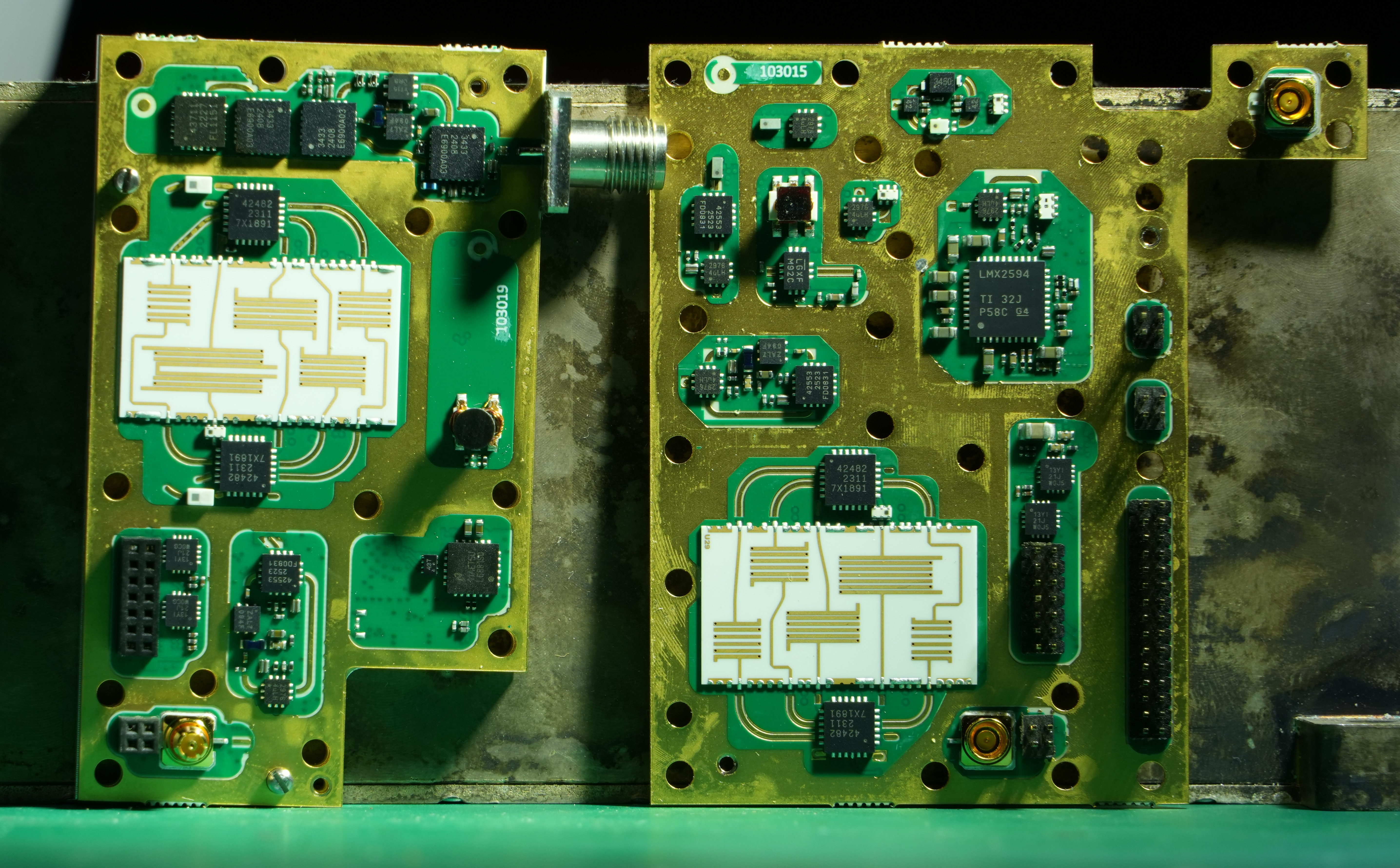
The RF signal path begins at the front-panel SMA connector on PCB 1 (left board in the paired view).
RF PCB 1 (Input Stage)
Key observations:
- The input signal is routed through a network of:
- RF switches
- Step attenuators
- Amplifier stages
- A dedicated low-frequency path is present, routed through a balun, suggesting a separate LF signal chain
- After the switching network, a prominent filter bank is implemented
- The processed signal is then transferred to PCB 2 via a board-to-board connector
RF PCB 2 (Pre-Mixer Stage)
- A ceramic substrate filter is used, with passband characteristics closely matching those on PCB 1
- The filtering topology appears to use a cascaded or differential-like configuration, combining multiple filter sections to achieve finer selectivity
- The filtered RF signal is fed into the first mixer stage
Adjacent to the mixer is a Texas Instruments LMX2594 wideband PLL/VCO synthesizer, serving as the local oscillator (LO).
Notably, multiple RF switches are placed around the first mixer. These switches enable:
- Multiplexing between up-conversion and down-conversion modes
- Reuse of a single mixer IC across different frequency ranges
This topology reduces component count and PCB area while maintaining functional flexibility.
The resulting first intermediate frequency (IF) signal is then routed to the next stage via another board-to-board connector.
IF Processing and Frequency Conversion (PCB 3)
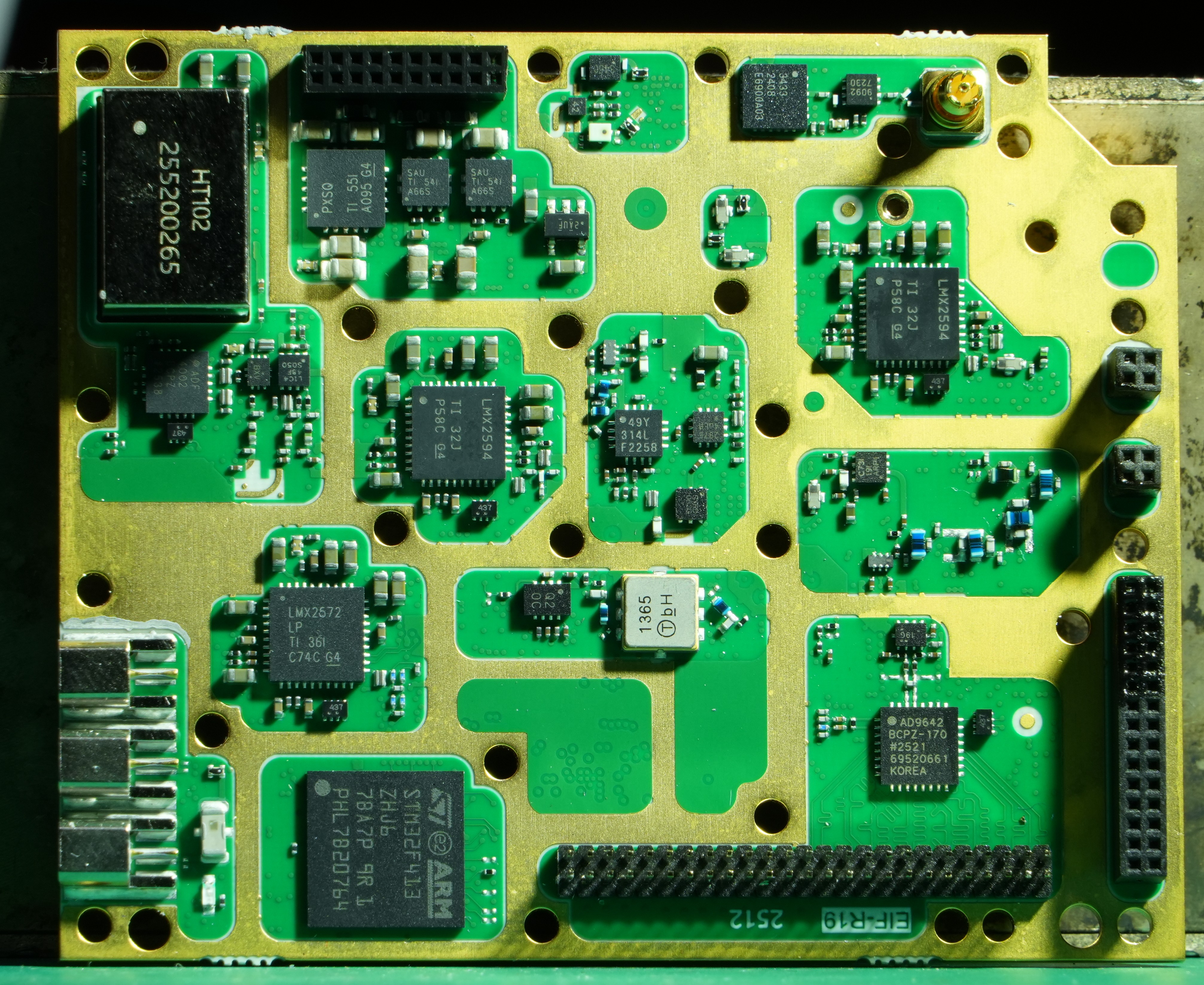
The third PCB contains additional frequency conversion stages.
Two additional LMX2594 synthesizers are present, indicating that the SAN-45 employs a triple-conversion superheterodyne architecture.
This approach is common in compact, cost-optimized designs, as it shifts image rejection and spurious suppression requirements into the IF domain, reducing reliance on high-performance RF preselection filters.
Notable Features
- Two LMX2594 synthesizers generate the second and third LO signals
- IF filtering is implemented using a combination of:
- Ceramic (TLCC-type) filters
- SAW filters
- Discrete LC filters
The inductors in the LC sections are arranged orthogonally, minimizing mutual coupling—an indicator of careful RF layout practice.
A precision crystal oscillator and associated clock distribution circuitry occupy a dedicated area. These components play a critical role in achieving the specified phase noise performance.
Digital Processing and Interface (PCB 4 / FPGA Board)
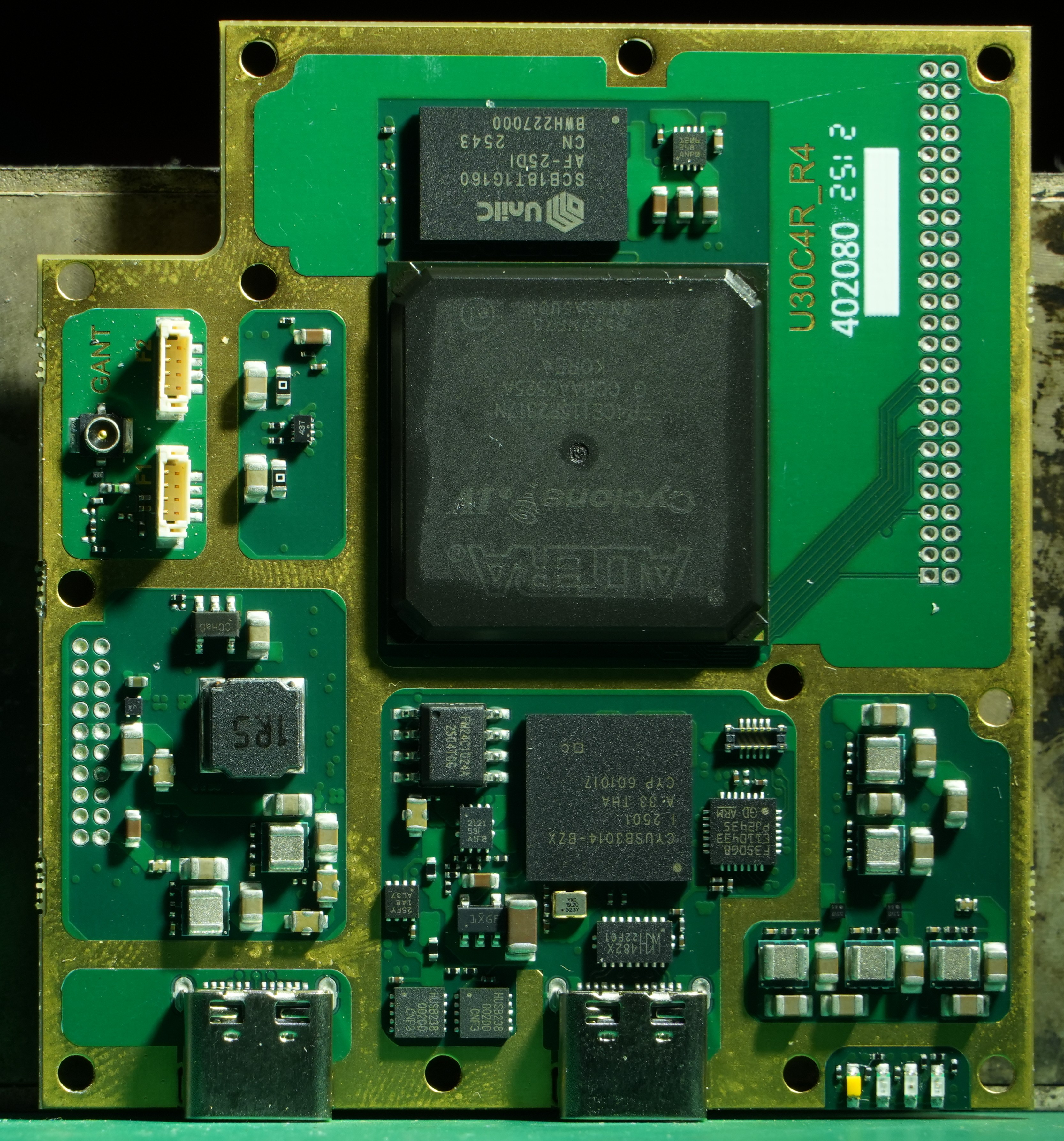
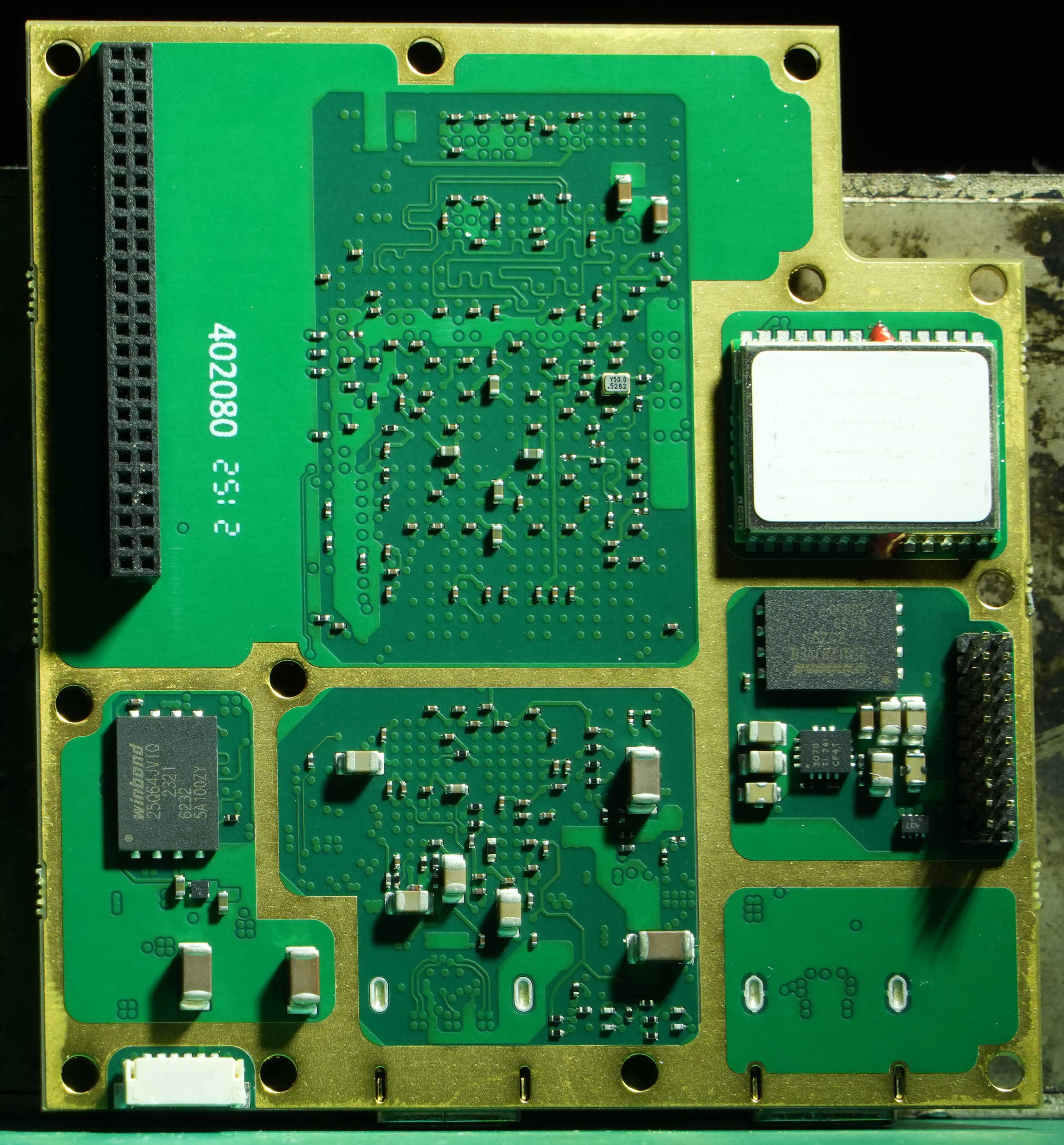
The final board in the stack handles digital processing.
- Built around an Altera (Intel) Cyclone-series FPGA
- Responsible for real-time DSP operations, likely including:
- FFT processing
- Trace processing and detectors
- Triggering functions
- Data formatting and streaming over USB
- A GNSS (GPS) module is also present, providing disciplined clock capability
This separation between RF/IF processing and digital processing is consistent with modular instrument design practices.
Design Approach Summary
The SAN-45 follows a classical triple-conversion superheterodyne architecture, combined with extensive use of RF switching for signal path and LO reuse.
Key design characteristics include:
- Emphasis on compact integration
- Use of multi-stage frequency conversion to balance performance and cost
- Heavy reliance on RF switching networks for flexibility
- Implementation of layered IF filtering using a mix of TLCC, SAW, and LC filters
- Robust thermal management to support stable operation
Within its price class, this architecture represents a practical trade-off between performance, complexity, and cost, complemented by software features that enable a wide range of measurement functions.
Disclaimer
This analysis is intended for educational and engineering reference purposes only.
For official specifications, performance data, and technical support, please refer to Harogic’s documentation and SAStudio4 software.
The product is currently available on the Deepace website.